- 您现在的位置:买卖IC网 > Sheet目录126 > CDBFN140-G (Comchip Technology)DIODE SCHOTTKY 40V 1.0A SOD323
发布紧急采购,3分钟左右您将得到回复。
 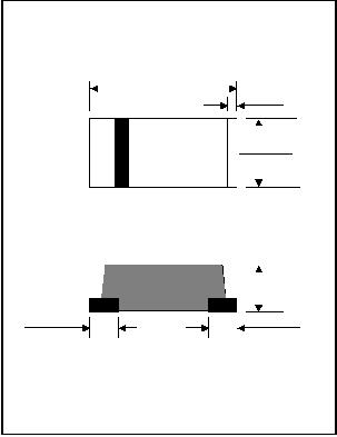    V oltage: 20 to 100 Volts Current: 1.0 Amp RoHS Device Page 1 REV:E CDBFN120-G Thru. CDBFN1100-G Dimensions in inches and (millimeter) QW-BB022 SOD-323 SMD Schottky Barrier Rectifiers Comchip Technology CO., LTD. 0.012(0.3) Typ. 0.016(0.4) Typ. 0.016(0.4) Typ. 0.106 (2.70) 0.091 (2.3) 0.057 (1.45) 0.041 (1.05) 0.047 (1.2) 0.031 (0.8) Parameter Symbol CDBFN CDBFN CDBFN CDBFN CDBFN CDBFN CDBFN 120-G 130-G 140-G 150-G 160-G 180-G 1100-G Unit Repetitive peak reverse voltage Maximum RMS voltage Continuous reverse voltage Maximum forward voltage @IF=1.0A Forward rectified current Forward surge current, 8.3ms half sine wave superimposed on rated load (JEDEC method) Typ. thermal resistance, junction to ambient air Typ. diode junction capacitance (Note 1) Operating junction temperature Storage temperature VRRM VRMS VR VF IO IFSM IR RθJA CJ TJ TSTG 1.0 30 0.5 10 90 120 -55 to +125 -55 to +150 V V V V A A mA O C/W pF O C OC Note 1: f=1MHz and applied 4V DC reverse voltage. -65 to +150 20 14 20 30 21 30 40 28 40 50 35 50 60 42 60 0.55 0.70 80 56 80 100 70 100 0.85 Reverse current on VR=VRRM @TA=25 O C @TA=125 O C Maximum Ratings (at TA=25°C unless otherwise noted) Features Mechanical data -Case: JEDEC SOD-323, Molded plastic -Terminals: Solde plated, solderable per MIL-STD-750, method 2026. -Polarity: Indicated by cathode band. -Mounting position: Any -W eight: 0.008 gram(approx.). - Batch process design, excellent power dissipation of fers better reverse leakage current. -Low profile surface mounted application in order to optimize board space. -Low power loss, high ef ficiency. -High current capability , low forward voltage dorp. -High surge capability . -Guardring for overvoltage protection. -V ery iny plastic SMD package. -Ultra high-speed switching. -Silicon epitaxial planarchip, metal silicon junction. -Lead-free parts meet environmental standards of MIL-STD-19500 /228 |
| *型号 | *数量 | 厂商 | 批号 | 封装 |
|---|---|---|---|---|
|
|
添加更多采购
